
What Every Microelectronics Startup Needs: A Checklist of Critical Equipment
 Microelectronics, the backbone of our digital age, is a field where innovation is constant, and the stakes are high. For startups venturing into this exciting space, the journey is exhilarating but fraught with challenges. A key hurdle is acquiring the right equipment. We need the tools that turn raw materials into the intricate circuits that power our devices.
This article provides a checklist of essential equipment for microelectronics startups. Whether you’re making a groundbreaking sensor or a new chip, this checklist will help you choose the right equipment.
Wafer Processing and Cleaning Equipment
Wafer processing equipment is key to semiconductor fabrication. It turns raw wafers into intricate circuits. But, the importance of ultra-clean wafers for successful fabrication cannot be overstated. Contaminants, even at the microscopic level, can wreak havoc on the delicate processes that follow.
Various cleaning methods, such as wet chemical cleaning and dry cleaning, are used to remove impurities. However, as a startup, if in-house cleaning isn’t feasible, professional services offered by companies like Silyb Wafers can be helpful. Such companies specialize in wafer polishing, cleaning, and metrology and have helped many clients. They can also be a valuable asset to your business.
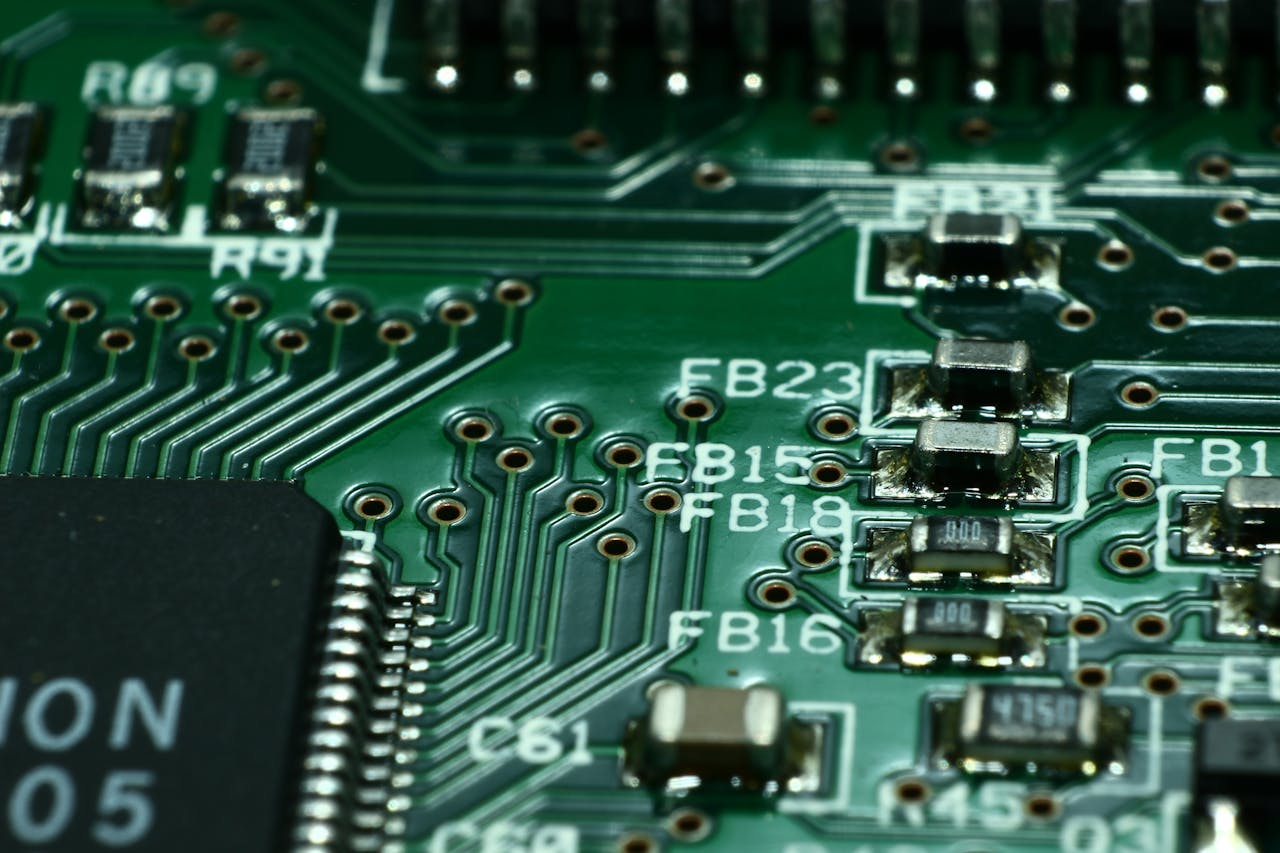
Metrology and Inspection Tools: The Eyes of Quality Control
Metrology and inspection tools are essential for ensuring the quality and precision of wafer fabrication. They act as vigilant eyes, overseeing every step of the process.
Microscopes (Optical, Electron)
High-resolution imaging is crucial in microelectronics, where dimensions are miniscule. Optical microscopes provide detailed views of the wafer surface. They reveal patterns, defects, and any irregularities that could impact performance.
Electron microscopes, with their superior magnification, delve deeper. They allow engineers to examine the intricate structures of the semiconductor at the atomic level. Identifying and addressing these microscopic flaws is essential for reliable and functional devices.
Profilometers: Measuring the Invisible
Profilometers measure what’s invisible to the naked eye: film thickness and surface roughness. These measurements are vital for wafer integrity. They ensure that deposited layers conform to design specifications.
Film thickness variations can affect electrical properties. Excessive surface roughness can lead to adhesion issues. Profilometers provide precise data. Engineers use it to fine-tune the fabrication process and maintain high quality.
Must-Have Equipment for Every Startup
Beyond the core wafer processing tools, supporting equipment is key. It helps maintain a smooth and efficient fabrication process. These unsung heroes ensure a clean environment, accurate measurements, and seamless device testing.
A Controlled Environment
Microelectronics fabrication demands an ultra-clean environment to prevent contamination. Cleanrooms have HEPA filters to remove airborne particles. They also maintain a controlled temperature and humidity. Air showers and specialized garments worn by personnel further minimize the risk of contamination.
Test and Measurement Equipment
Once devices are fabricated, their electrical characteristics need to be thoroughly tested. Test and measurement equipment like oscilloscopes, spectrum analyzers, and parameter analyzers help engineers verify that the devices function as intended. These tools give insights into the components’ electrical behavior. They allow adjustments to the fabrication process.
Probing Stations
Probing stations let engineers contact individual devices on a wafer for testing. These stations have micromanipulators and probes. They can precisely connect to the device’s tiny pads. Engineers can test a device by applying electrical signals and measuring the responses. This helps them find performance issues.
Additional Considerations
Beyond the core and supporting equipment, a few additional considerations are vital for a successful microelectronics startup.
Masks: The Blueprint for Success
Masks are the master templates that define the patterns on a wafer. These intricate designs are transferred onto the wafer during photolithography.
Different mask types, such as binary and phase-shift masks, offer varying levels of complexity and resolution. Selecting the right mask material, like chrome or quartz, is also crucial for achieving the desired results.
Software Tools: Designing and Simulating
Software tools play a crucial role in every stage of microelectronics fabrication. Computer-Aided Design (CAD) software is used to create the intricate layouts of the devices. Simulation tools help predict the behavior of the devices under various conditions.
This allows engineers to optimize designs before fabrication. Data analysis platforms help interpret these test results. This further leads to a better fabrication process.
Calibration and Maintenance: Ensuring Peak Performance
Regular calibration and maintenance are essential for keeping equipment in top condition. Calibration ensures accurate measurements, while maintenance prevents unexpected breakdowns and costly delays. Establishing a robust maintenance schedule is crucial for maintaining consistent production and high-quality results.
Takeaway
Equipping a microelectronics startup is a multi-faceted endeavor. This checklist is a roadmap. It guides you to the key tools for wafer processing, the supporting equipment, and other considerations like masks and software.
Remember, each startup is unique. Tailor this checklist to your specific needs and budget. With the right tools and a plan, your microelectronics venture can thrive in this dynamic industry.


Leave a Reply
Want to join the discussion?Feel free to contribute!